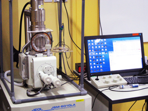
CRADLΣ has an analytical scanning electron microscope that is available for student research projects. Unlike pure service facilities, we want students to operate the instrument themselves and gain the first-hand experience.
Read on to learn more
-
PART I
History
The first electron microscope (EM) was developed in 1931 by German physicist Ernst Ruska (1986 Nobel prize in physics) and is an adaptation of traditional optical microscopes, with light being replaced by an electron beam and optical lenses replaced by electromagnetic “lenses”.
The Scanning Electron Microscope (SEM) was invented by German physicist Manfred von Ardenne around 1937, and may be considered a direct outgrowth of the then rapidly advancing television technology: it is very much an adaptation of a television camera electron tube.
Since then, both EM and SEM have evolved tremendously, and in particular, the SEM is today a standard research workhorse. Modern SEMs are so easy to use that they are often preferred even if a conventional optical microscope would be sufficient to do the job!
Operating Principle
In an SEM, a narrow beam of fast-moving electrons is generated by an “electron gun”. The beam is then shaped and focused onto a tiny spot on the sample, using a system of apertures and electromagnetic lenses. The “response” of the sample is then measured. By steering the electron beam to another spot, a different response may be obtained. This process is repeated in a systematic way, and a “map” of the response of different sample regions is assembled pixel-by-pixel – the SEM image is formed.
There are many different types of “response” that can, in principle, be tested. The two most common ones are:Backscattered electrons:
The electron beam is largely absorbed by the sample, but since negatively charged electrons are attracted to positively charged nuclei, some may “swing around” a nucleus of the sample and “bounce back”, similar to a comet being flung back into space after swinging by the sun. These backscattered electrons can be detected.
Because the backscatter process depends on the positive charge of nuclei, chemical elements with a higher atomic number (higher nuclear charge) give rise to a stronger response. In this way, an SEM backscattered electron image (BEI) gives not only information about the shape of the sample but also hints at what elements microscopic features of the sample may be made from.
Secondary electrons:
The sample, being made from atoms, already contains a large number of electrons. When the electron beam impinges on the sample, some of the sample's electrons may “splatter” out of the sample. This is called secondary electron emission and is quite similar to water droplets splashing out of a pail if one aims a water jet at it. The secondary electron image (SEI) generally provides better image quality than BEI.
CRADLΣ's electron microscope can provide both BEI and SEI images.
-
PART II
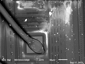
SEI vs BEI example:
Left: Detail of an ancient silicon chip contaminated by dust in SEI mode.
Right: Same sample in BEI mode. The dust specks appear much brighter against the silicon chip in the background, indicating that they contain much heavier elements.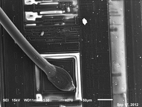
Elemental Analysis via X-Ray Spectroscopy
When a sample is hit by the SEM's high-energy electron beam, it emits x-ray radiation. Each chemical element has its own characteristic x-ray spectrum; by measuring the spectrum emitted by any point on the sample, one can find out what chemical elements are present. This technique is known as energy-dispersive x-ray spectroscopy (EDS or EDX). Because the electron beam can be focused at will on different regions of the sample, differences in the composition of microscopic features can be investigated.
CRADLΣ's electron microscope is equipped with an EDX accessory.EDX example:
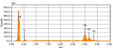
Left: Sub-micrometer detail of the embossed data track of a computer DVD.
Right: The EDX spectrum of this sample shows that the reflective metal film is made from silver (Ag). The carbon (C) and oxygen (O) peaks arise from the polycarbonate plastic substrate beneath the thin metal film.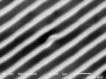
-
PART III
SEM and Optical Microscope Compared
- The resolution (detail) seen in an SEM is much better than that of a conventional optical microscope.
- SEM resolution depends on the type of sample and other factors, but CRADLΣ's electron microscope generally achieves resolutions on the order of tens of nanometres.
- The resolution of conventional optical microscopes is limited to hundreds of nanometres; however, a typical resolution limit (without resorting to immersion optics, phase contrast techniques etc.) is about 1 micrometre.
- Suitability for non-flat samples
- Conventional optical microscopes have working distances (distance between object and objective lens) of about a millimetre, and the depth of field (distance range over which a sharp image is obtained) is very small. This makes it difficult to work with non-flat samples.
- SEMs have much larger working distances (10 mm and more) and a very large depth of field. This makes it much easier to observe 3-dimensional samples and also allows tilting the sample to change the viewing angle.
- The electron beam in an SEM must travel in a vacuum.
- The sample must be able to withstand a vacuum.
- Volatile samples (that evaporate or sublimate) are not suitable for SEM.
- This generally rules out “wet” samples, such as fresh biological tissue.
- Wet samples can be dried, but users should be aware that the drying process may cause artefacts (the sample may shrivel, crack, or change its appearance in other ways).
- The electron beam interacts with the sample at or near the surface
- Unlike optical microscopy, the sample cannot be covered by or embedded in a transparent material.
- The negative electric charge from the electron beam may accumulate on a sample
- The sample should be conductive to allow draining this charge. Otherwise, strong image artefacts can result.
- Non-conductive samples can be coated with a thin conductive layer, but this can also cause artefacts.
- CRADLΣ's electron microscope also allows BEI operation in a “low vacuum” mode that can often eliminate the need for coating non-conductive samples. (SEI operation in low vacuum mode is not possible.)
- The sample may be damaged by the intense electron beam
- As the sample is hit by high-energy electrons that can easily break chemical bonds, radiation damage may occur.
- Apart from radiation damage, the electron beam also causes the sample to heat up, i.e. the sample may be charred.
- Electron beams are deflected by magnetic fields
- The SEM may not work well if the sample is magnetised.
- SEMs are quite complex machines.
- SEMs require more training than a conventional optical microscope.
- Damage caused by carelessness or lack of understanding can be very expensive.
- The resolution (detail) seen in an SEM is much better than that of a conventional optical microscope.
-
FAQ
What are the typical applications of the SEM?
Morphological and elemental characterisation of natural and man-made micro- and nanostructures, micro-/nanoparticles, failure and forensic analysis, crystallites, (dry) biological specimen, ...
What SEM model does CRADLΣ have?
CRADLΣ has a JEOL JSM-6100LA.
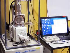
What are that weird grey cage and the protruding coils for?
These are components of an electronic system that cancels interfering magnetic fields and improves the performance of the SEM. This system was built by a 17-year-old SAYES member during a two-month research attachment at CRADLΣ!
What are the principal capabilities of the SEM?
SEI, BEI, EDX, high and low vacuum modes; variable acceleration voltage up to 20 kV; full sample tilt/rotate capability; in situ live video camera; optical stage navigation system.
Who can use the CRADLΣ SEM?
Students of MOE schools, for bona fide student research projects.
Where can students learn how to use the SEM?
CRADLΣ arranges training sessions as needed.
What kind of conductive coating is available for nonconductive samples?
CRADLΣ uses a gold sputter coater.
Does CRADLΣ have a critical point drier?
At this time, no.
How can I book the SEM?
Contact us via email at cradle@science.edu.sg, and provide as much information as possible concerning the type of sample and nature of work. Usage charges are listed here.


.jpg)


